Getting Thermal Imaging Right in Your Wafer Tools
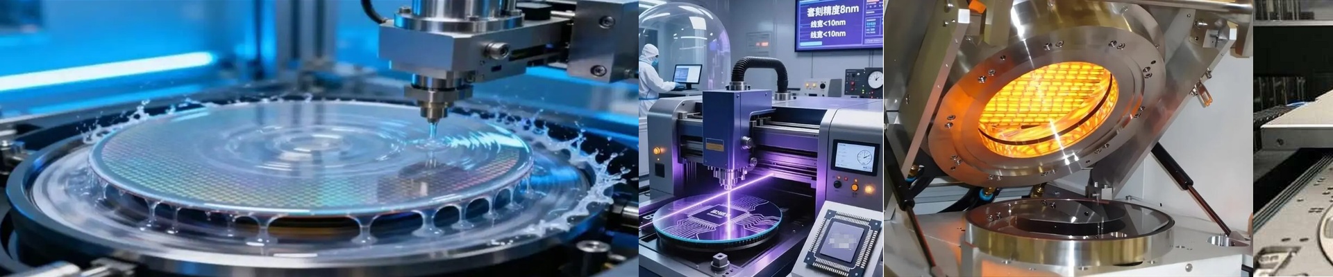
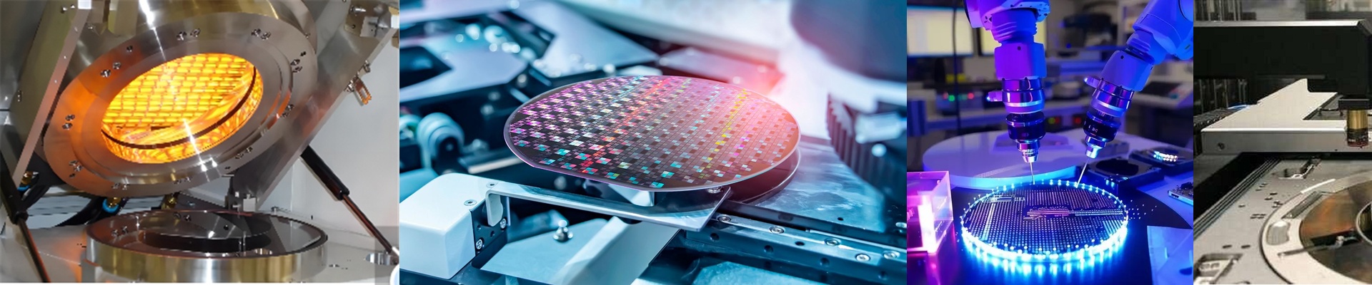
If you’re trying to move toward a smarter Fab, you’ve probably realized that old-school contact thermometers just don’t cut it anymore. They’re slow. And honestly? Touching the wafer is a risk you don’t need to take. That’s why we’ve shifted to high-speed infrared (IR) systems. We can grab real-time thermal maps without ever touching the surface. No contamination, no mechanical stress—just clean data.
Stop guessing, start seeing
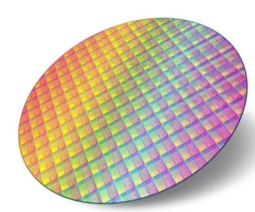
Digital production is all about the data stream. We plug IR sensors directly into your PLC or SCADA system, turning heat radiation into digital signals instantly. Here’s the best part: you’re finally seeing theactual wafer surface. With thermocouples, you’re often just guessing based on the Temperature of the susceptor or the chamber wall. Now, you get a direct look. If something drifts on that 300mm surface, you’ll know immediately and can tweak your heating elements on the fly.
Dealing with the “Window” problem
Vacuum chambers are brutal environments. The biggest headache is usually the “window effect”—where the quartz or sapphire viewing ports basically block the IR signal. It’s frustrating, but we’ve found a way around it. We calibrate our sensors to hit specific wavelength bands that slide right through those materials. Just a heads-up: keep your optical path clean. If outgassing residues start building up a film on the window, your readings will start to drift. It’s a simple fix, but it’s the difference between a perfect run and a wasted wafer.
The trade-off
The upside is huge for your tool design. You can ditch those bulky probes and reclaim some serious space in the chamber. It feels much leaner. But there is a catch. High-res IR sensing pumps out a lot of data. If you’re scaling this across a whole fleet of tools, make sure your network backbone can handle it. If the data lags, your PID loop lags. And in advanced node manufacturing, a millisecond of latency is a luxury you can’t afford.